Anyone even slightly familiar with electronics knows the NE555 IC. This almost iconic timer circuit was designed in the summer of 1971 by Hans R. Camenzind, a Swiss-born electrical engineer who taught at Northeastern University in Boston. Yes, we’re the same age! It’s not the “greatest” IC because it’s the largest in size or the most advanced in capability, but because it was probably manufactured in the largest quantity. In some years, one billion units were sold, most of them produced by Samsung in Korea. Before his death in 2012, Hans Camenzind stated that the internal design of the NE555 was not particularly elegant, and that it should have been redesigned decades earlier. While elegance might be important to an engineer, for the user, affordability, practicality, and versatility are more important — and it is thanks to these qualities that the NE555 achieved its unparalleled success.
According to legend, the type number came from the pre-printed labels used in the lab where the development was done — they had >>NE5 _ _<< printed on them. This led to serial numbers like 567, 568, and so on. However, the marketing guy, Art Fury, somehow sensed that this project would be a big hit and suggested assigning it the number 555, because it would be easier to sell.

(Source: www.transistormuseum.com)
The IC contains 25 bipolar transistors, 2 diodes, and 15 resistors on a silicon chip in an 8-pin DIP package. The prototype was manufactured in October 1971, and by the summer of 1972, 12 major electronics companies were already producing it. It became the most successful integrated circuit of all time. Later, a dual version appeared under the model number NE556 in a 16-pin package (containing two full NE555 circuits), followed by low-power CMOS versions such as the Intersil ICM7555 or the Texas Instruments LMC555. A version containing four timers was also made under the model number NE558.
The circuit can be used in astable mode as an oscillator, as a monostable timer, or as a bistable flip-flop. It’s not limited to timing applications — enthusiastic designers have built thousands of other circuits with it, from water level switches for tanks to battery chargers. Numerous books have been published featuring NE555 circuit “recipes”; one of the best, in my opinion, is IC Timer Cookbook by Walter G. Jung, published in 1977. I can also recommend Colin Mitchell’s free e-book 50 555 Circuits.
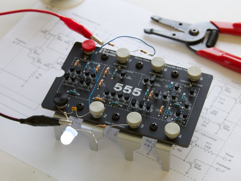
You can build all sorts of things with the NE555, but who on earth would think of building the NE555 itself? Well, at Evil Mad Scientist Laboratories, it was Eric Schlaepfer who designed a $35 kit that lets you assemble a functional NE555-equivalent circuit out of discrete transistors — on a board shaped like an 8-pin DIP package (though, of course, much larger).

It’s a great gadget for beginners to learn from. It’s also a fun project — very cool! And it makes a great gift for geeks, too. Of course, it has no real practical use, since it’s big and expensive — a real NE555 costs around $0.15 (~30 forints).
You can buy this gadget here: https://shop.evilmadscientist.com/productsm…/tinykitlist/652

It’s great for educational purposes, since with a real NE555 you can only access the pins, but with this one, you can take measurements inside the “IC” while it’s operating.

In the picture, those little black thingies are the transistors. The internal structure of a real NE555 integrated circuit is only visible under a microscope — and at first glance, it doesn’t seem all that interesting:

The yellowish lines are metallic conductor tracks. Beneath them lies a thin, glassy silicon dioxide layer that serves as insulation. At the openings in this layer, the conductive tracks connect to the silicon die underneath. Specific regions of the silicon die are treated with doping elements, creating what’s known as n-type and p-type semiconductor regions — the fundamental building blocks of any such integrated circuit. In circuit diagrams, a transistor is usually represented by a single symbol, while textbooks sometimes illustrate it as being made of three semiconductor layers. Something like this:

C stands for collector, B for base, and E for emitter. This is an NPN transistor because it consists of two n-type and one p-type layers. If you don’t yet understand how a transistor works, for now it’s enough to know that it’s a kind of switch: the current applied to the base controls (or switches) the current flowing between the collector and the emitter.
Now, in reality, the internal structure of a transistor inside an IC is a bit more complex than the simplified diagrams found in textbooks. For example, one of the transistors in the NE555 looks like this under a microscope, viewed from above, and like this in a simplified cross-sectional side view:

On the chip, this small region can do exactly the same thing as those little round black thingies in the Evil Mad Scientist kit — except those are individually encased in plastic, while here, many transistors share a single substrate and are encased together in one package. That’s what makes it an integrated circuit.
Note: Sometimes transistors need to handle higher currents. In such cases, their size is increased. In the image above, the three structures in the corners that resemble towel warmers are higher-power transistors. The two on the left are the output transistors, and the one in the lower right is the discharge transistor (pin 7). The dark “fly-leg” structures on the edge of the image are the bonding wires that connect to the external pins.
Now I’m just wondering when someone will get the idea to build a microprocessor out of discrete transistors? Say, the Intel 4004 (1971), which had only about 2,500 transistors — compared to the Core i7 humming under this desk, with its 3.2 billion transistors!
(VidG’s note: someone actually started building a 4004 out of TTL logic gates — see: https://gigatron.io)
NE555 Circuit Examples
For anyone who has some basic knowledge of electronics, is interested in the topic, but doesn’t yet know this IC, I’d like to share a few thoughts about how it works.

The NE555 is an extremely robust and versatile device. It can be used in bistable, monostable, and astable timer modes — for various delay functions, as a pulse generator, in alarm circuits, sound generators, for controlling LEDs and strobe lights, etc. One of its key features is that the timing intervals are practically independent of supply voltage and temperature, and are quite accurate — at least for an RC timer. Of course, it’s nowhere near as precise as a quartz oscillator, so don’t try to build an atomic clock with it!
The Texas Instruments NE555 datasheet can be downloaded here (PDF)
The block diagram of the NE555 is shown in the figure below. At the heart of the circuit is the R-S flip-flop and two comparators (marked in orange as 1 and 2). The three 5 kΩ resistors form a voltage divider between ground and the supply voltage. This divides the supply voltage into thirds: comparator 1’s (+) input receives 1/3 Vcc, and comparator 2’s (–) input receives 2/3 Vcc. (So for example, if the IC is powered from 9 V, those voltages are 3 V and 6 V.)
Note: Comparators share the same schematic symbol as an operational amplifier and an op-amp without feedback can be used as a comparator, but it work very differently. Comparators have a digital output which can only put out a HIGH or a LOW, very near to the power supply rails. If the positive (analog) input is greater than the negative (analog) input (even by a few millivolts), the digital output goes HIGH. Likewise, the digital output is LOW when negative input is higher than the positive input. Note that the positive/negative inputs do not indicate a positive or negative voltage, but the difference in voltages on the two inputs.
Inside the 555 there are two comparators. This comparators compare the voltages on the Trigger and Threshold inputs to these reference voltages. Comparator 1 outputs a logic high when the voltage on the Trigger input is lower than 1/3 Vcc. When this happens, the S (Set) input of the flip-flop is activated, the flip-flop is set, and the output switches to high. If the voltage on the Threshold input exceeds 2/3 Vcc, comparator 2 activates the R (Reset) input of the flip-flop, causing it to reset — and the output goes low.
The flip-flop also has an independent reset (clear) input, connected to pin 4. This input overrides everything else: if pin 4 is pulled low, the flip-flop is cleared regardless of the other inputs, and the output (pin 3) goes low.
Note: A flip-flop is a digital logic device that has complementary outputs controlled by two inputs. The type of flip-flop used in the 555 is called an RS flip-flop. When the S (SET) input goes HIGH, the Q output goes HIGH and the Ǭ output goes LOW. It has a sort of one-bit memory, in that the S pin can return to a LOW or toggle many times, but the flip-flop “remembers” the last state and the outputs remain unchanged. When the R (RESET) input goes HIGH, the opposite happens. The Q output goes LOW and the Ǭ output goes HIGH.

- Pin 1: Ground
- Pin 2: Trigger
- Pin 3: Output
- Pin 4: Reset
- Pin 5: Control Voltage — reference from the internal voltage divider, 2/3 of the supply voltage
- Pin 6: Threshold
- Pin 7: Discharge — open-collector output, in phase with pin 3
- Pin 8: Supply Voltage (Vcc) — typically 3–15 V, maximum 16 V
The internal circuitry of the IC, broken down transistor by transistor, looks like this:

Note: You can get a 555 IC in both single and dual packages. The dual versions usually have the part number 556 in them. Many manufacturers still make it in 8-pin and 16-pin DIP packages for easy breadboarding.
Limitations
- The original bipolar version has a power supply lower limit of 4.5V, so you can’t use it in 3.3V circuits. The CMOS version works fine down to 2V.
- The theoretical maximum operating frequency for an NE555 timer can be around 500 kHz, but a practical maximum frequency for stable and predictable operation is often 100 kHz to 300 kHz depending on the manufacturer and layout. The CMOS version goes up to around 1.5 MHz.
- The bipolar version has a maximum output current capability of 200 mA, which it can sink or source, but this is a limit that should not be constantly exceeded to prevent overheating or damage to the device. While the 555 can supply this much current, it is generally good practice to draw only the minimum current needed by the load to ensure reliable operation and longevity. However, if you need more current than this, use a BJT or MOSFET transistor tied to the Out pin to boost current.
- CMOS 555 timers like the LMC555 or TLC555 have a much lower, non-symmetrical output current capability than the bipolar NE555. They typically have a sink capability of around 100 mA and a source capability of only about 10 mA. This is more than enough to drive most common LEDs or relay coils.
Bistable Multivibrator
With the following circuit, you can try out how the flip-flop works! In the default state, the Trigger input (pin 2) is pulled up to the supply voltage by resistor R1. When button S1 is pressed, the input drops to 0 V (which is less than 1/3 Vcc = 3 V), causing the flip-flop to set. A positive voltage appears on pin 3, which drives current through resistor R5 and LED2 — so LED2 lights up. LED1 remains off, because pin 3 is now near the supply voltage, and there’s virtually no voltage difference between the positive terminal of the 9V battery and pin 3.
(Those with a sharp eye and a bit of digital electronics experience may notice that the flip-flop’s Q’ (not Q) output is connected to pin 3 — so it should technically behave the opposite of what’s described. However, the output driver stage inverts the signal again, so in effect it behaves as if Q were connected.)

When button S2 is pressed, +9 V is applied to the Threshold input (pin 6), which was previously held at 0 V by resistor R2. This causes the flip-flop to reset: LED2 turns off, and LED1 lights up.
The circuit assembled on a breadboard looks like this:

Monostable Timer
So far, we haven’t seen how the NE555 actually functions as a timer. Suppose we want to control a staircase light — the goal is for the light to turn on when a button is pressed (via a relay, for example), and then automatically turn off after a certain amount of time. This can be achieved using the NE555 by replacing S2 and R2 in the previous circuit with a timing network — that is, a resistor and a capacitor:

Up until now, we haven’t mentioned pin 7 (Discharge). As seen in the block diagram above, this pin is connected to a transistor inside the IC, which is controlled by the output of the flip-flop. When the flip-flop is in its default (reset) state, this transistor is conducting, connecting pin 7 directly to ground. This effectively shorts capacitor C1. Even though current flows through resistor R2, capacitor C1 cannot charge — the voltage on pin 6 remains low (at ground level).
When button S1 is pressed, the flip-flop sets as described earlier. As a result, the output at pin 3 goes to +9 V (LED2 lights up), and the internal discharge transistor turns off. Capacitor C1 then begins to charge through resistor R2. Its voltage gradually increases until it reaches 2/3 Vcc = 6 V. At that point, comparator 2, which is connected to pin 6, switches state and resets the flip-flop. The timing interval has ended, the output at pin 3 goes low, and the internal discharge transistor connected to pin 7 discharges the capacitor. The circuit returns to its initial state and is ready to be triggered again.
The circuit looks like this when assembled on a breadboard:

This circuit is not retriggerable — that is, pressing the S1 button while the timing cycle is active has no effect; it won’t restart or extend the timing interval. Pressing S1 only has an effect once the timing has completed; only then can a new timing cycle be initiated. However, by adding a single diode, the circuit can be made retriggerable:


In this case, the S1 switch — in addition to triggering the timing through the Trigger input (pin 2) — performs the same function as the internal discharge transistor: it discharges capacitor C1 through diode D1. So, when the button is pressed during an ongoing timing cycle, it doesn’t affect the flip-flop inside the IC, but by discharging the capacitor, it restarts the timing process. The timing interval is now about 5 seconds. For example, if the button is pressed after 4 seconds, the timing restarts from zero, resulting in a total duration of 4 + 5 = 9 seconds. If D1 is not included, pressing S1 at the 4-second mark has no effect, and the timer stops after 5 seconds.
The length of the timing interval depends on the values of resistor R2 and capacitor C1. The formula was given above next to the schematic, but the nomogram below can also be used to determine the timing values:

As you can see, the same time interval can be achieved using different combinations of resistance and capacitance — we have many options to choose from. In practice, C1 typically ranges between 0.001 µF and 100 µF, while R2 can be selected anywhere between 1 kΩ and 10 MΩ. If we want to select from multiple timing intervals within a circuit, we can use several resistors and switch between them with a selector switch. Another option is to replace R2 with a variable resistor (potentiometer). These two methods can also be combined:

Astable Multivibrator
It’s logical to omit the S1 switch and connect the Trigger input directly to the capacitor. To allow discharging, we add another resistor. In this configuration, the capacitor charges through resistors R1 and R2 up to 2/3 Vcc, then discharges through R2 toward pin 7 down to 1/3 Vcc. The capacitor voltage oscillates between 6 V and 3 V, and the two comparators toggle the flip-flop back and forth. The LEDs blink alternately — this is the astable multivibrator circuit.


The timing intervals can now be calculated using the following formulas:
Charge time:
t₁ = 0.693 × (R1 + R2) × C1 = 0.693 × (47,000 Ω + 47,000 Ω) × 0.0001 F ≈ 6.5 sec
Discharge time:
t₂ = 0.693 × R2 × C1 = 0.693 × 47,000 Ω × 0.0001 F ≈ 3.3 sec
Total period:
T = t₁ + t₂ = 9.8 sec
Blinking frequency:
f = 1 / T ≈ 0.1 Hz
The output voltage at pin 3 (yellow waveform) and the capacitor voltage (green) appear like this on the oscilloscope screen in astable mode:

Since R1 + R2 is greater than R2, the charging time is always longer than the discharging time (t₁ > t₂). This circuit cannot produce a 50% duty cycle — a perfectly symmetrical square wave. The key to generating a symmetrical waveform is to charge and discharge the capacitor through two equal resistors. By adding diode D1, the charging current flows through resistor R1 and bypasses R2 via the diode. During discharge, the capacitor discharges through R2 toward pin 7. Since R1 = R2, the two half-periods will be equal in duration.

Another way to achieve a symmetrical square wave output is by not using pin 7 (Discharge) at all, omitting resistor R1, and connecting the upper end of resistor R2 directly to pin 3 (the output). In this setup, both charging and discharging happen through R2, not from the supply voltage, but from the output itself.
Siren
So far, I haven’t mentioned pin 5. This pin is connected to the upper part of the internal reference voltage divider, meaning it gives access to 2/3 Vcc — and it can also be externally influenced (more on this later). If it’s not used, it’s typically connected to ground through a 10 nF capacitor for noise suppression, as shown in the previous circuits.
The following circuit uses two NE555 ICs. IC1 is the symmetrical astable multivibrator we already know. The second one is a simpler astable circuit, but here its pin 5 (the reference voltage) is modulated by the output of the first stage — which causes its frequency (i.e., the pitch of the sound) to vary in sync with the oscillation of the first stage:
